TELECENTRIC GREEN LASER MARKER SAMPLES
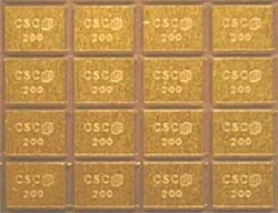
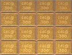
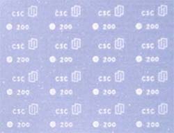
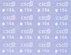
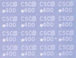
Laser Marking on 6 inch arrays with over 2000 sections of ~1mm x ~1mm semiconductor. Each marking containing two lines of text, and the ability to include a logo. It was required to mark on 2 different surfaces, epoxy and gold plated.
 |
 |
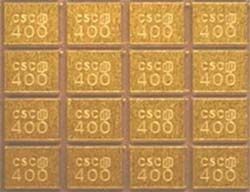 |
| Gold Plated Wafer - 200 μm Text | Gold Plated Wafer - 300 μm Text | Gold Plated Wafer - 400 μm Text |
 |
 |
 |
| Epoxy Wafer - 200 μm Text | Epoxy Wafer - 300 μm Text | Epoxy Wafer - 400 μm Text |
| Copyright © Custom Systems and Controls, Inc. | Privacy Policy | Contact Us | |
|